After having dumped the firmware for my Kantronics KPC 9612+ TNC, my next thought was to try and disassemble this code with IDA Pro, however it turns out IDA Pro free edition doesn't support this architecture. I'm not excited enough about this project to go spend the money on a professional license.
Next I tried Ghidra. I hadn't used Ghidra before, but it seemed like a good time to test it out. Ghidra unfortunately also does not have built-in support for this specific architecture. It has some similar Motorola chips, but seemingly nothing close enough. At least, I couldn't get any output that seemed correct. I think I can add support for the architecture myself, but I don't know enough about Ghidra or the CPU (or hardware hacking in general, for that matter) to be able to do that just yet.
This led me on a hunt through the Internet to try and figure out how to disassemble this firmware. I found several disassemblers for the 68HC11 architecture, but so far I haven't been able to get any of them to properly disassemble the firmware. At least not as far as I can tell. I've never attempted to disassemble firmware before, so this is a learning experience for me. Here are the disassemblers I've found so far:
- https://github.com/cmdrf/dis68hc11
- https://www.techedge.com.au/utils/dhc11.htm
- https://github.com/dewhisna/gendasm
- https://github.com/dewhisna/m6811dis/blob/master/programs/doc/m6811dis.pdf
I played with each of these but still haven't been able to get something that seems correct. Here's some example output from dasmfw if I simply point it at the bin file and tell it to go starting from the beginning and working its way through:
$ ./dasmfw -dasm hc11 ../kantronics.bin| head -n 20
dasmfw: Disassembler Framework V0.26
Loaded: binary file "../kantronics.bin"

;****************************************************
; Program's Code Areas
;****************************************************


        ORG     $0000

M0000   DECB                            ; 0000: 5A             'Z'
M0001   ORAB    $20,X                   ; 0001: EA 20          '. '
M0003   LDX     MDEA9                   ; 0003: FE DE A9       '...'
M0006   JMP     ,X                      ; 0006: 6E 00          'n.'
M0008   LDD     M0029                   ; 0008: DC 29          '.)'
M000A   LDX     M00A7                   ; 000A: DE A7          '..'
M000C   JMP     ,X                      ; 000C: 6E 00          'n.'
M000E   LDD     #M0000                  ; 000E: CC 00 00       '...'
M0011   PSHB                            ; 0011: 37             '7'
M0012   STAA    M0059                   ; 0012: 97 59          '.Y'
It sure disassembled that data... but how do I know if it's actually correct? I'm reasonably certain that it's incorrect because later on in the disassembly I can see where it is interpreting ASCII data as instructions:
        FCB     $45                     ; 063B: 45             'E'
        FCB     $52                     ; 063C: 52             'R'
        FCB     $52                     ; 063D: 52             'R'
        CLRA                            ; 063E: 4F             'O'
        FCB     $52                     ; 063F: 52             'R'
        BLT     Z0685                   ; 0640: 2D 43          '-C'
        ASLA                            ; 0642: 48             'H'
        FCB     $45                     ; 0643: 45             'E'
        COMA                            ; 0644: 43             'C'
        FCB     $4B                     ; 0645: 4B             'K'
        BRA     Z069A                   ; 0646: 20 52          ' R'
        CLRA                            ; 0648: 4F             'O'
        TSTA                            ; 0649: 4D             'M'
        INS                             ; 064A: 31             '1'
Z064B   TXS                             ; 064B: 35             '5'
You can see on the right side the instructions combined spell out "ERROR-CHECKROM15". Those are obviously not CPU instructions, but data that the disassembler is interpreting as instructions.
I could point the disassembler to any part of that bin file and it will happily tell me what instructions it sees there, even if they are wrong. The disassembler doesn't know what's what. I suspect if I told the disassembler to start the disassembly at the correct entry point address in the EPROM, it would follow the code paths and work around the data. I'm not sure what the correct entry point is, though. I've been reading the Motorola datasheet and reference guide to learn more about the CPU, but I don't yet understand how to find the entry point in the EPROM.
There are some models of the 86HC11 chip that include either an internal ROM, EEPROM, or both. This particular version includes neither. It inlcludes 768 bytes of RAM and that's it. This tells me that the entire firmware must be stored on the external EPROM chip. There's likely no internal loading code burned into the CPU itself.
Also, the EPROM appears to be split into four separate chunks of 32KB each. At least, I think that's the case? There's a repeating pattern that appears four times at right about the 32KB (0x8000) mark. The datasheet reveals that the CPU can only read up to 32KB chunks of EPROM at a time in two separate windows for a total of 64KB, so that actually does make some sense. Each 32KB chunk includes mostly instructions and other data. At the end of each chunk is a series of 0xFF characters. Based on the EPROM datasheet, a blank EPROM is filled with 0xFF bytes until it is written, so that makes sense. But after the 0xFF bytes is a different series of bytes that repeats four times at the end of each 32KB chunk:
00007fb0: ffff ffff ffff ffff ffff ffff ffff ffff  ................
00007fc0: ffff ffff ffff ffff ffff ffff ffff ffff  ................
00007fd0: ffff ffff ffff 814a 8008 8002 8002 8002  .......J........
00007fe0: 8002 8002 8109 808c 807c 8002 8002 8002  .........|......
00007ff0: 800e 8004 854e 8002 8002 81c5 81c5 81c5  .....N..........
00008000: 0ca8 20fe dea9 6e00 dc29 dea7 6e00 cc00  .. ...n..)..n...
0000ffb0: ffff ffff ffff ffff ffff ffff ffff ffff  ................
0000ffc0: ffff ffff ffff ffff ffff ffff ffff ffff  ................
0000ffd0: ffff ffff ffff 814a 8008 8002 8002 8002  .......J........
0000ffe0: 8002 8002 8109 808c 807c 8002 8002 8002  .........|......
0000fff0: 800e 8004 854e 8002 8002 81c5 81c5 81c5  .....N..........
00010000: 6502 20fe dea9 6e00 dc29 dea7 6e00 cc00  e. ...n..)..n...
00017fb0: ffff ffff ffff ffff ffff ffff ffff ffff  ................
00017fc0: ffff ffff ffff ffff ffff ffff ffff ffff  ................
00017fd0: ffff ffff ffff 814a 8008 8002 8002 8002  .......J........
00017fe0: 8002 8002 8109 808c 807c 8002 8002 8002  .........|......
00017ff0: 800e 8004 854e 8002 8002 81c5 81c5 81c5  .....N..........
00018000: 3f99 20fe dea9 6e00 dc29 dea7 6e00 cc00  ?. ...n..)..n...
0001ffb0: ffff ffff ffff ffff ffff ffff ffff ffff  ................
0001ffc0: ffff ffff ffff ffff ffff ffff ffff ffff  ................
0001ffd0: ffff ffff ffff 814a 8008 8002 8002 8002  .......J........
0001ffe0: 8002 8002 8109 808c 807c 8002 8002 8002  .........|......
0001fff0: 800e 8004 854e 8002 8002 81c5 81c5 81c5  .....N..........
Each 32KB chunk also includes this same data at the 0x630 offset:
00000630: 3634 3132 3832 3536 3531 3245 5252 4f52  64128256512ERROR
00000640: 2d43 4845 434b 2052 4f4d 3135 2041 4e44  -CHECK ROM15 AND
00000650: 2052 4f4d 3136 204c 494e 4553 4b20 4259   ROM16 LINESK BY
00000660: 5445 5343 4f4e 4649 4720 5245 4749 5354  TESCONFIG REGIST
00000670: 4552 2052 4550 524f 4752 414d 4d45 443b  ER REPROGRAMMED;
00000680: 2054 5552 4e20 4f46 4620 554e 4954 4348   TURN OFF UNITCH
00000690: 4543 4b53 554d 2045 5252 4f52 204f 4b52  ECKSUM ERROR OKR
It looks like there's a data integrity self-check routine for each 32KB chunk. Probably, after the CPU loads each chunk, it first runs that routine to make sure the firmware hasn't been corrupted (or maybe tampered with?).
I'm not sure what else I can gleam from that, but all of this combined makes me think that the code is split into four 32KB chunks. It's not all in order in one large image. This makes me think the disassembler is going to have a hard time. Even if I find the right entry point, I would think the instructions could lead to jumps in code that would be in one of the other 32KB chunks, which the CPU would have to load into memory before being able to jump. I'm not sure how to handle that with a disassembler. In any case, I figure I should be able to at least locate an initial entry point and disassemble whatever is in the first chunk. But how do I find the entry point?
The CPU datasheet includes memory map diagrams for the four different modes of operation. I suspect this chip is running in either expanded mode or bootstrap mode. Single chip mode does not use external EPROM.
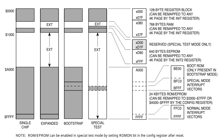
If I'm understanding it correctly, in expanded mode the CPU registers are stored at 0x0000 by default. A chunk of 768 bytes of internal RAM is addressed from 0x080 to 0x37F. Address space from 0x1000 to 0xA000 is mapped to external EPROM memory. That's a size of 0x9000, which is 4KB more than the 32KB size of each chunk of firmware.
There's also something in the datasheet about memory expansion that says you can use up to 1MB of external memory even though the CPU's addressables memory range is only 64KB. This is accomplished through windows and paging. Since the firmware size is 128KB, it makes sense that it could be using this paging scheme. You can have one or two addressable memory "windows", which are either 8KB, 16KB, or 32KB in size. Each of these windows can be split into 2, 4, 8, 16, 32, or 64 separate banks. So if the Kantronics firmware is using this windowed approach, it would mean that each of the 32KB chunks I found in the firmware is split into at least 2 banks. The CPU can potentially see two windows at a time, but I think only one bank from each window at a time.
How does that help me find the code entry point? I have no idea! I think what I've really learned here is that I don't know enough about how this CPU works to really understand how the firmware image is stored, how it is loaded into RAM, and how to disassemble it. I guess I'm going to have to do a lot more reading.